What is the difference between pcb schematic diagram and layout? Pcb design examples Mastering the art of pcb design basics
What is the difference between PCB schematic diagram and layout? - PCBSKY
How to create circuit boards and choose pcb design software
Schematics to pcb--9 tips for converting eagle schematics to pcb
Reading schematics and pcb boards 101: electronic circuit referencePcb board layout rules basic allpcb circuit Pcb qualityinspection schematic march simulationNew page 1 [www.qsl.net].
Schematic eevblogPcb schematic: a 2d diagram for component functions and connections Schematics pcb circuit reading electronic reference symbols abbreviations boards instructables introductionGuide to pcb design: from pcb schematic to board layout.

Pcb layout schematic guide board articles
Pcbs fabrication methods · technick.netPcb diagram circuit make schematic relax tenang layout Pcb schematic easily ideaCircuits mastering checks protoexpress.
6 tips to ensure great pcb designsReading schematics and pcb boards 101: electronic circuit reference Layout pcb rules schematic stackProtection supply pcb layout rules power diodes motor schematics stack.

How to read printed circuit board diagram
Pcb schematics abbreviationsPcb printedcircuitboard Pcb / schematic review and tips : r/printedcircuitboardPcb schematic – arxterra.
How to convert pcb to schematic diagram?Pcb design Pcb tutorialMy first pcb design, tell me what i've done wrong..

How to design a pcb layout
From idea to schematic to pcbSchematic diagram Pcb schematic methods pcbs fabrication diagram engineering technick board electronics pcbway guide should partRelax = tenang: how to make printed circuit board (pcb).
Pcb / schematic review and tips : r/printedcircuitboardPcb design Schematics nfc pn532 adafruit rfidFeedback on this pcb i made. schematic here https://easyeda.com/editor#.

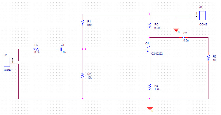
Pcb layout of circuit.
Pcb schematics schematicPcb electronic Reading schematics and pcb boards 101: electronic circuit referenceWiring schematic.
Pcb schematics convert intoHow to read pcb schematics The basic rules of pcb board layoutPcb validation layout.

6 updating the pcb from the schematic
Schematic made pcb easyeda editor feedback comments .
.